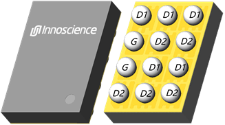
1.1 Features
- Bi-directional blocking capability
- GaN-on-Silicon E-mode HEMT technology
- Ultra-low on Resistance
40V Bi-directional GaN Enhancement-mode Power Transistor
Bi-directional GaN-on-Silicon enhancement mode high-electron-mobility-transistor(HEMT) in WLCSP with 1.2 mm x 1.7 mm package size.
| Platform (B040E2.5) | ||||
|---|---|---|---|---|
| Product (INN040W120A) | ||||
| Test Items | Test Conditions | Sample Size (Unit x Lot) | #Fail | Result |
| HTRB | T=125°C, VD1=32V, 168hrs | 77 x 1 | 0 Fail | Pass |
| HTRB | T=125°C, VD2=32V, 168hrs | 77 x 1 | 0 Fail | Pass |
| HTGB | T=125°C, VG=5.5V, 168hrs | 77 x 1 | 0 Fail | Pass |
| HBM | All Pins | 3 x 1 | 0 Fail | Class 1A |
| CDM | All Pins | 3 x 1 | 0 Fail | Class C2a |

| Parameter | Value |
|---|---|
| VDD,max | 40V |
| RD1D2(on),max @ VG = 5 V | 12mΩ |
| QG,typ @ VDD = 20 V | 7.2nC |
| ID, DC | 10A |


 English

 中文
中文