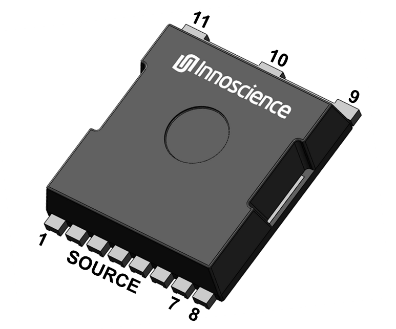
| Platform product (INN650TA030AH) |
|---|
| Test Items | Test Conditions |
Sample Size
(Unit x Lot)
| #Fail | Result |
|---|
| HTRB |
T=150°C, VDS= 560V |
77 x 3 |
0 Fail |
Pass |
| HTGB |
T=150°C, VGS= 7V |
77 x 3 |
0 Fail |
Pass |
| HTGB(-) |
T=150°C, VGS= -6V |
77 x 3 |
0 Fail |
Pass |
| LTRB |
T=-40°C, VDS= 650V |
77 x 1 |
0 Fail |
Pass |
| LTGB |
T=-40°C, VGS= 7V |
77 x 1 |
0 Fail |
Pass |
| LTGB (-) |
T=-40°C, VGS= -6V |
77 x 1 |
0 Fail |
Pass |
| TC |
-55 to +150°C, Air |
77 x 3 |
0 Fail |
Pass |
| HAST |
T=130°C, RH=85%, VDS=100V |
77 x 3 |
0 Fail |
Pass |
| H3TRB |
T=85°C, RH=85%, VDS=560V |
77 x 3 |
0 Fail |
Pass |
| HTS |
T=150°C |
77 x 3 |
0 Fail |
Pass |
| IOL |
ΔTj ≥ 100℃, Ton=Toff=2min |
77 x 1 |
0 Fail |
Pass |
| Solderability |
1. Precondition: 8H
2. Pb-free, 245±5°C, 5±0.5S. |
10 x 1 |
0 Fail |
Pass |
| HTOL |
Vplatform=450V,Irms=15A, Fre=65KHZ,Tj=125°C |
8sets x 3 |
0 Fail |
Pass |
| MSL3 |
T=30°C, RH=60%,3 x reflow |
25 x 3 |
0 Fail |
Pass |
| HBM |
All Pins |
3 x 1 |
0 Fail |
Class 2 |
| CDM |
All Pins |
3 x 1 |
0 Fail |
Class C3 |

 English
 简体
简体

