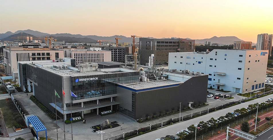
About INNOSCIENCE
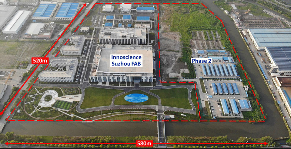
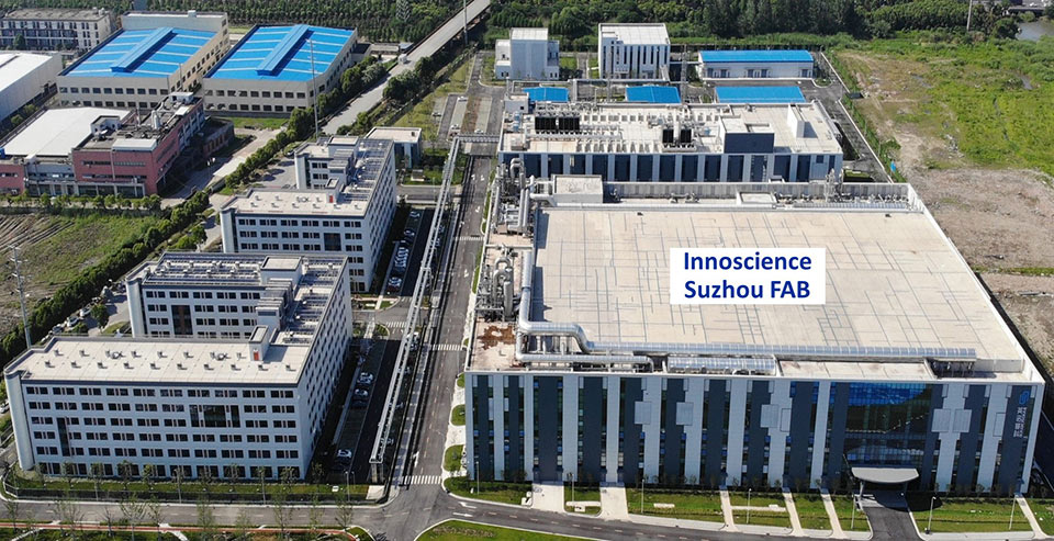
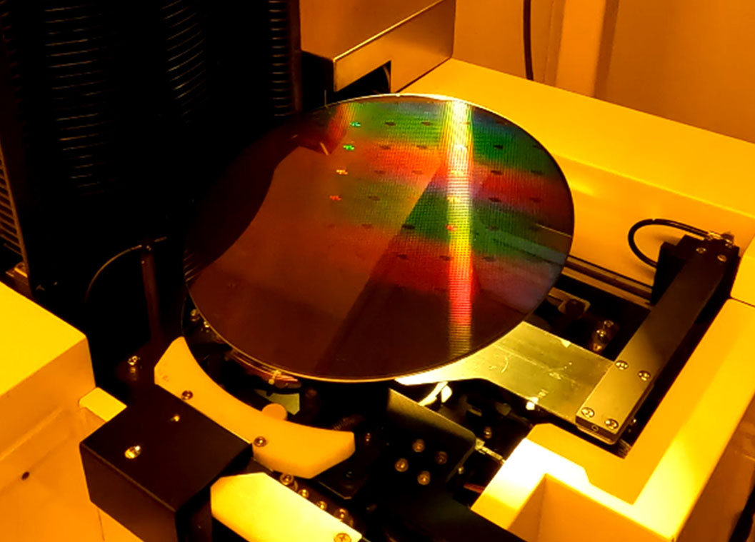
Innoscience is the largest 8-inch Integrated Device Manufacture (IDM) fully focused on GaN technology in the world. We fully control and own the world-wide largest dedicated 8-inch GaN-on-Si wafers manufacturing capacity.
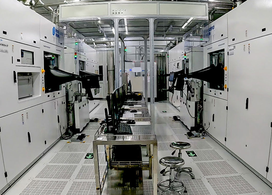
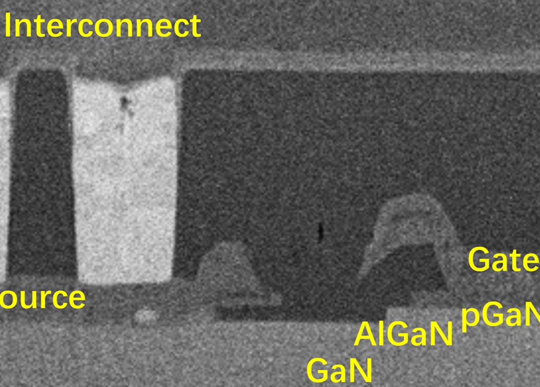
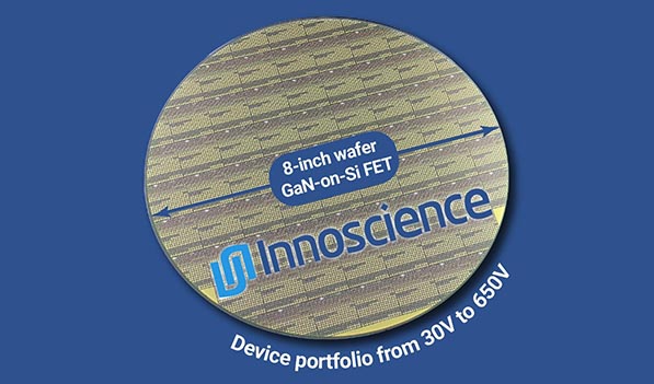
We design, develop and manufacture highly performing and reliable GaN devices for a wide range of applications and voltages (15V-900V). We assure excellent performance, reliability, support, security of supply, large capacity and lowest prices thanks to our large volume capabilities, 8-inch wafer size and advanced high-throughput manufacturing tools.
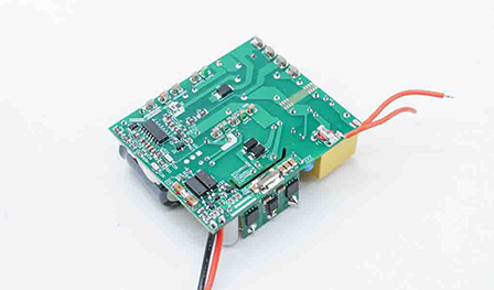
Innoscience’s GaN devices are already used in several products such as Power Delivery chargers, smart phones, laptops, LIDARs, Data centers etc. We collaborate with several customers and partners to enable systems and solutions based on GaN technology.

 English
 中文
中文


 News
News
 News
News
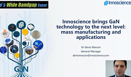
 Events
 News
News
 News
News
 News
News
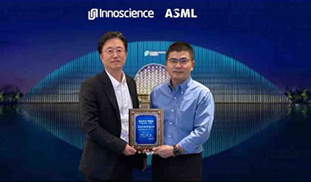
 Events
 News
News
 News
News
 News
News
 News
News
 News
News
 News
News
 News
News
 News
News
 News
News
 News
News
 News
News
 News
News
 News
News
 News
News
 News
News
 News
News
 News
News
 News
News
 News
News
 News
News
 News
News
 News
News
 News
News
 News
News
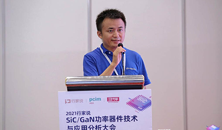
 Events
 News
News
 News
News
 News
News
 News
News
 Events
 News
News
 News
News
 Events